PCB Production Support
We are working with several PCB production facilities and can offer Cost-effective PCB production : from simple 2-Layer PCBs to High-Density and Exotic PCB production and Assembly services.
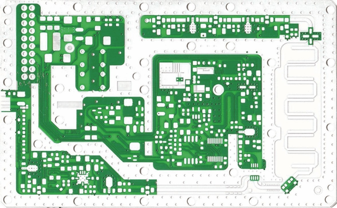
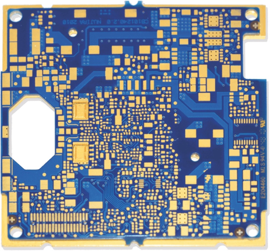
MICROWAVE PCBs
A distinctive feature of microwave printed circuit boards is a wide range of high-frequency signals that are distributed through strip lines of transmissions. This fact is reflected in the special features of the design of the microwave circuit boards and sets up special demands for the parameters of dielectrics and the quality of manufacture of the print pattern elements. In the manufacture of microwave printed circuit boards, high-frequency laminates are used. These materials are reinforced by glass fiber polymer and ceramic thermoset laminates with a little tangent of an angle of dielectric losses and a wide range of dielectric coefficients.
PCBs WITH EMBEDDED COMPONENTS
PCBs with embedded components are the most complex to manufacture. Special technologies allow us to include the lead-free chip components, uncased transistors, diodes, etc. inside of multilayer PCBs. It is also possible to create the structure of the resistive layers which allows forming thin-film resistors. The usage of embedded components can reduce the size and weight of the device, as well as increase reliability.
FLEXIBLE, RIGID-FLEXIBLE PCBs
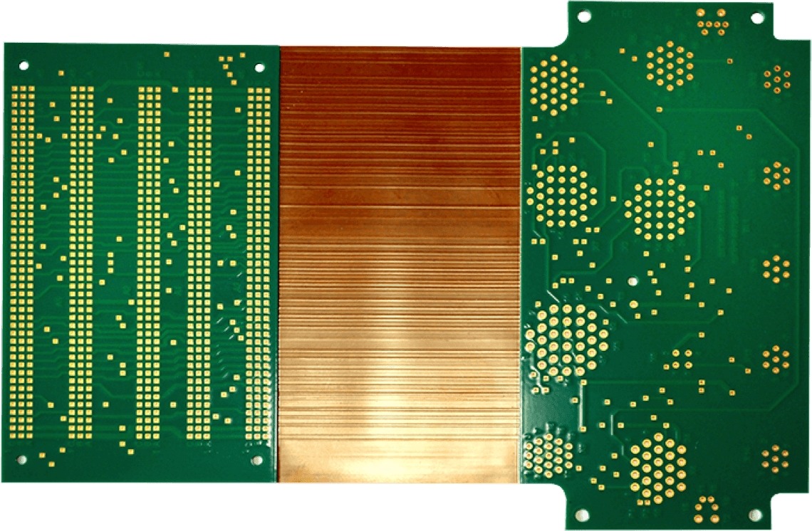
Flexible circuit boards (up to 8 layers) and flat flexible cables have significant advantages over traditional wired cables in complex devices, reducing assembling cost and allowing to connect of different connectors and components in different locations in 3D designs. The core materials are low thickness polyimide films and PET.
METAL CORE PCBs
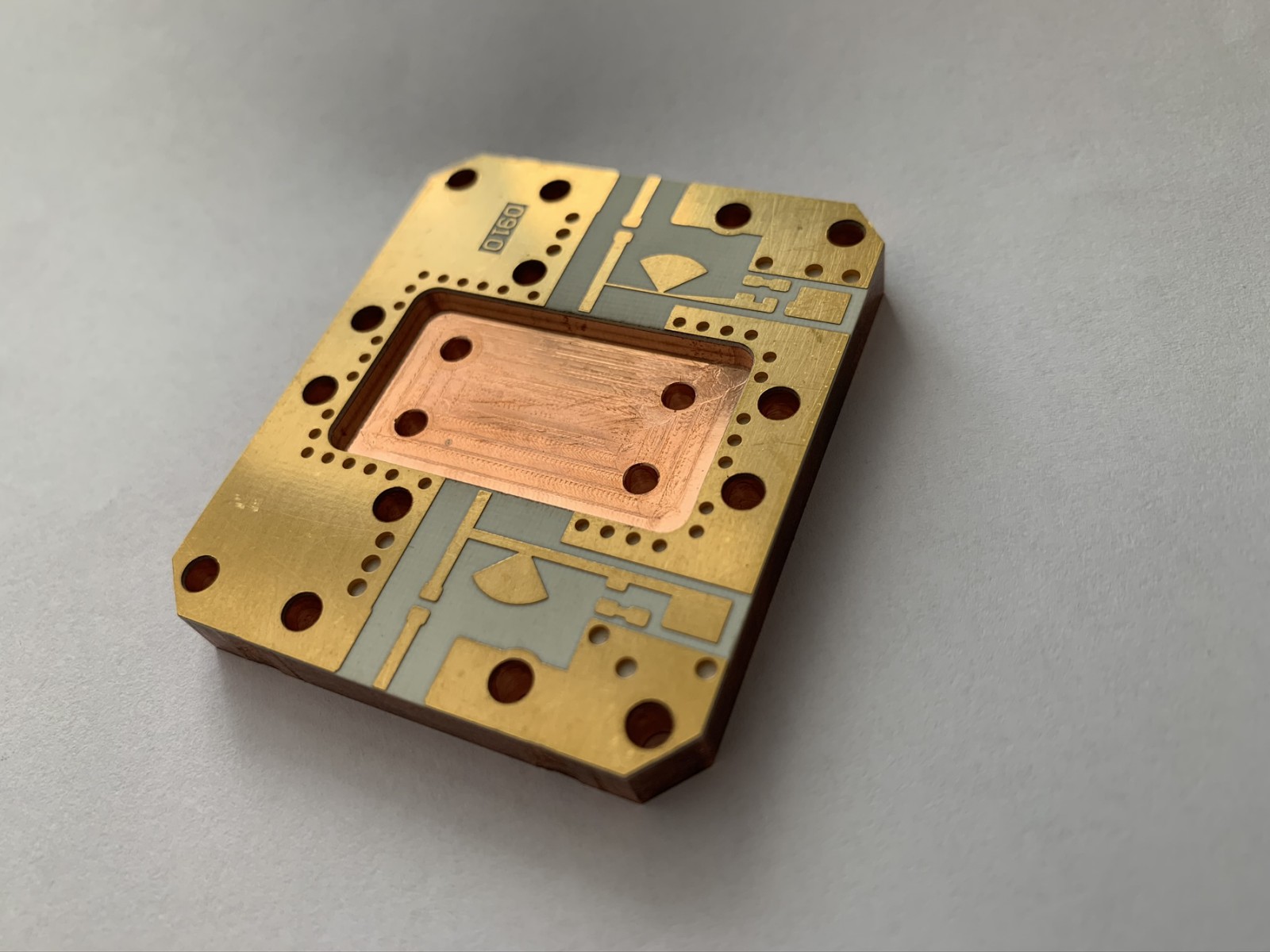
The main feature of the metal core printed circuit boards is a thick metal plate (such as Al, Cu, Fe) and thin dielectric with high thermal conductivity thus allowing to increase overall heat dissipation and easily attach the board to the heat sink.
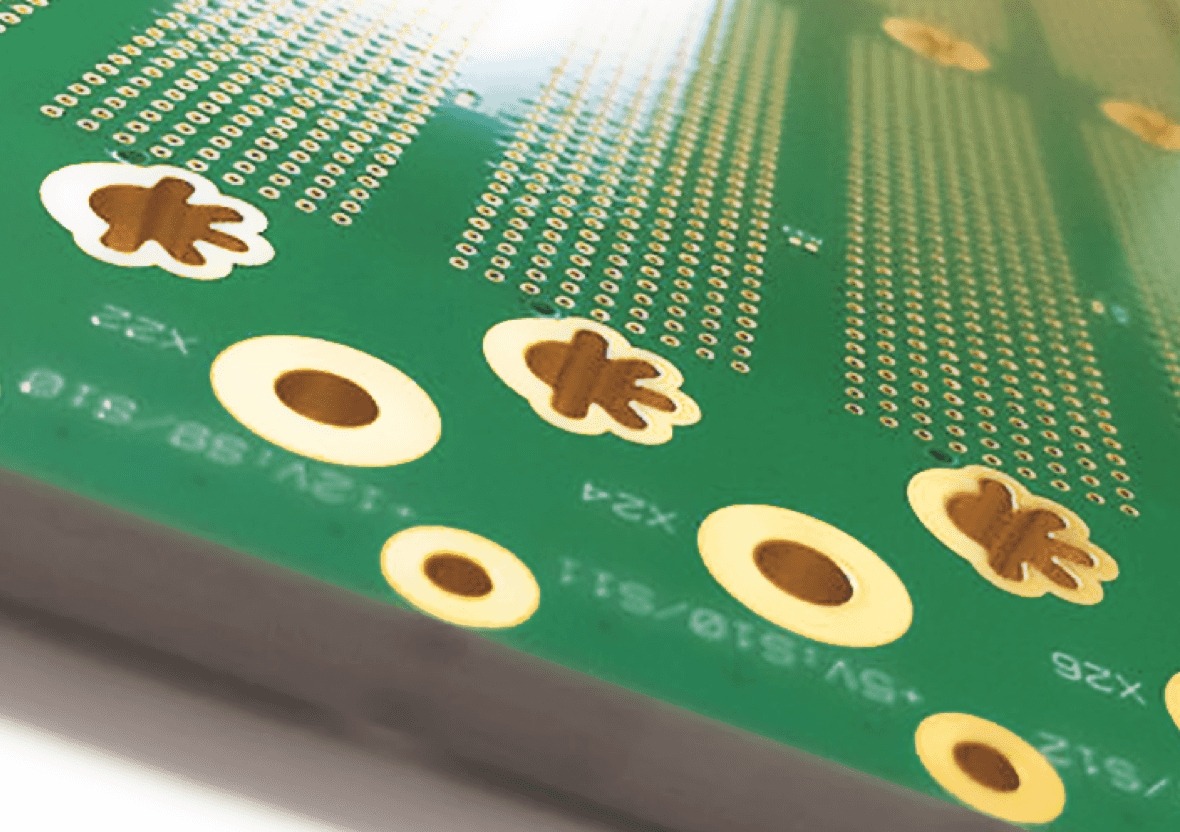
BACKPLANE PCBs
IMPEDANCE CONTROLLED PCBs
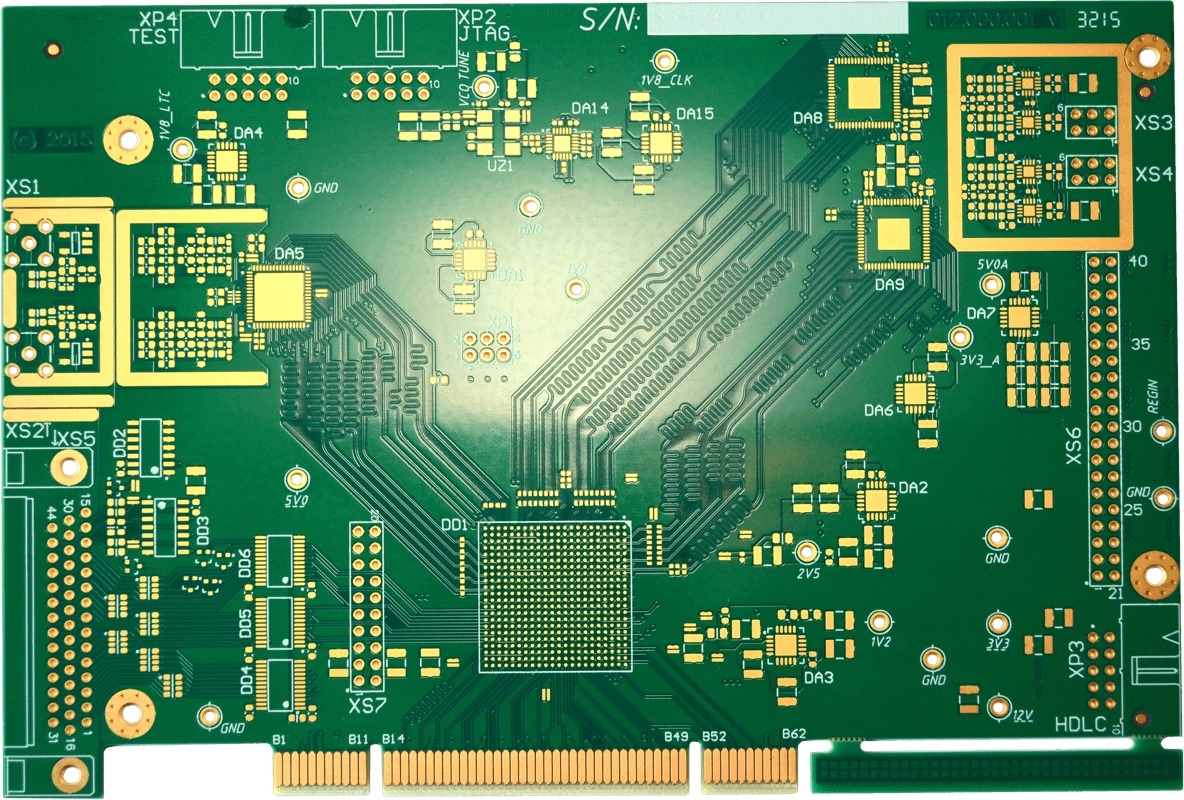
Impedance controlled printed circuit boards are manufactured of materials with high stable parameters. Special attention is paid to the board’s stack up, route patterns of transmission lines. It allows us to minimize the signal losses and provide high-speed data transmission.
PLANAR TRANSFORMERS
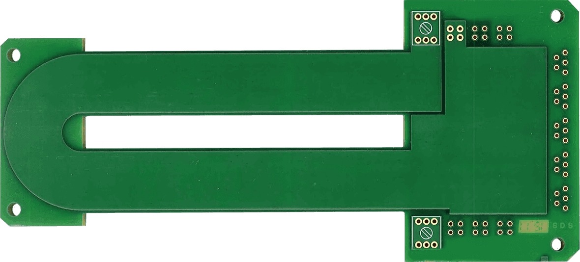
Using planar transformers minimizes the size of devices and improves design reliability. For the manufacturing of planar transformers, the dielectrics with high breakdown voltage and thick foil are used to maintain high currents and interlayer insulations.
HDI MULTILAYER PCBs
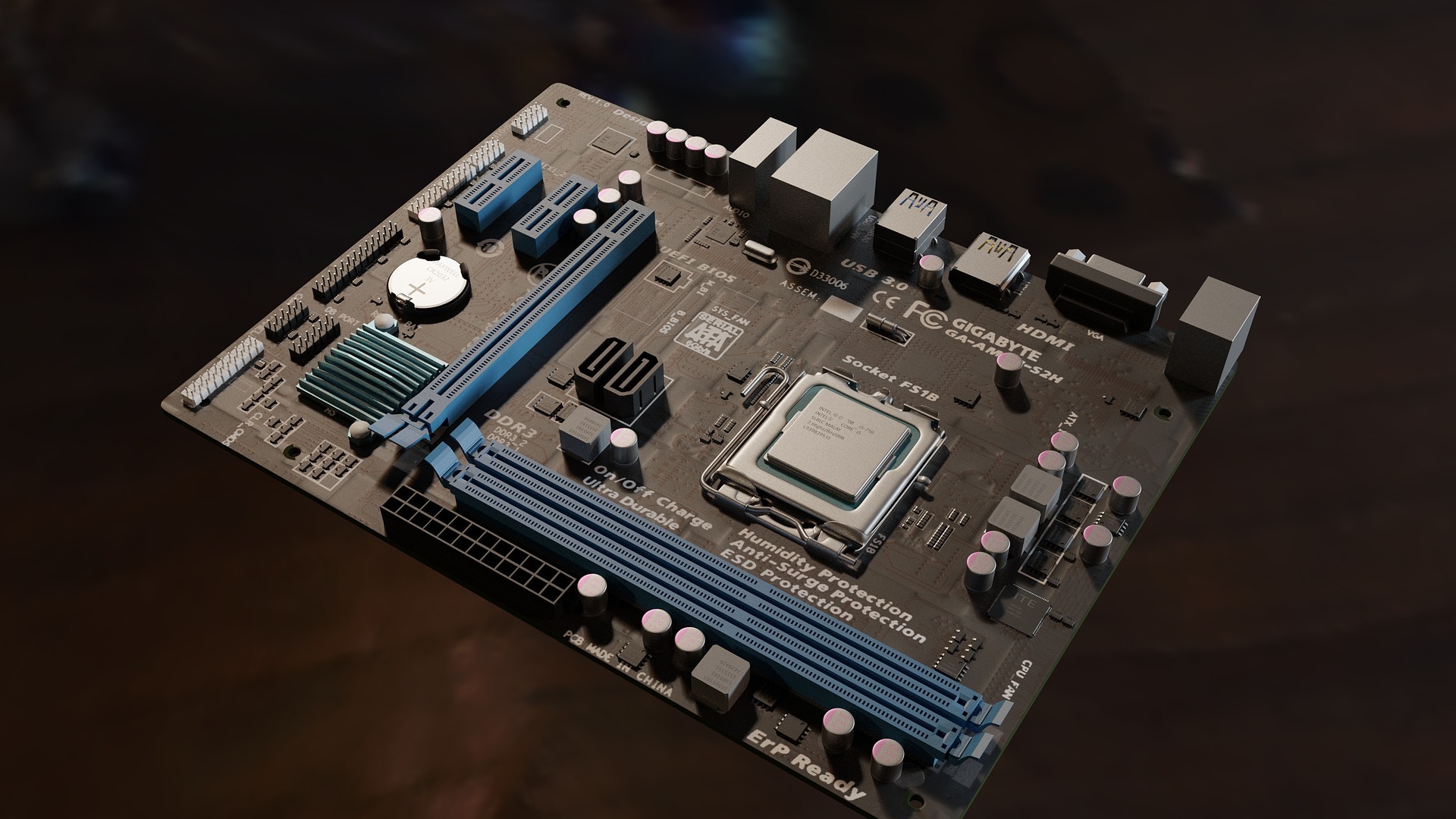
The highest quality basic materials, sophisticated manufacturing processes, and most advanced technologies are used for HDI printed circuit boards production. HDI PCB design has buried vias, blind laser micro vias, conductors width, and gaps under 100 um.
